


How thin can an LED display be, and which technology makes it possible?
Many buyers focus on pixel pitch, brightness, or refresh rate when evaluating LED displays. However, thickness has become a major purchasing factor in recent years. Retail brands want displays that blend into store architecture. Corporate clients want video walls that sit closer to the wall. Transportation operators need lighter screens to reduce structural load. As a result, manufacturers have developed new packaging technologies that significantly reduce display thickness.
This guide explains how thin modern LED displays can become, what limits display thickness, and how PCB, COB, and COG technologies differ. You will also learn the practical trade-offs behind ultra-thin designs so you can make smarter purchasing decisions.
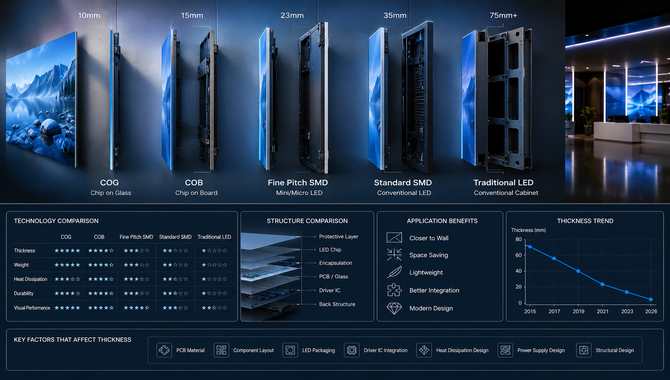
How Thin Can an LED Display Actually Be?
AIO Grab Block
Quick Answer
The thinnest commercial LED displays today use COG (Chip-on-Glass) technology and can achieve thicknesses below 10 mm. Traditional PCB-based LED displays typically range from 30–80 mm, while COB displays generally range from 15–35 mm depending on cabinet design.
| Technology | Typical Thickness |
| Traditional PCB LED | 30–80 mm |
| Ultra-Slim PCB LED | 20–35 mm |
| COB LED | 15–35 mm |
| COG LED | 5–10 mm |
| Future Micro LED Glass Display | <5 mm |
Modern LED displays can be thinner than a smartphone while still delivering commercial-grade brightness and durability.
However, buyers should understand that “display thickness” is often a marketing term. Some suppliers only measure the visible display layer. Others include the cabinet, power supply, mounting structure, and cooling system.
From a manufacturing perspective, we recommend evaluating the total installed depth rather than the panel thickness alone. A display that appears to be 8 mm thick may require a mounting structure that increases total installation depth to 40 mm or more.
Many projects do not actually require the thinnest available technology. A retail flagship store may benefit from a 10 mm display, but a conference room video wall often achieves the same visual result with a 30 mm solution at a lower cost.
Why Thickness Matters in Modern LED Projects
Display thickness affects more than appearance.
A thinner display typically weighs less, occupies less space, and integrates more easily into modern architecture. This becomes especially important in premium commercial environments where aesthetics directly influence customer perception.
For example, luxury retail brands increasingly prefer displays that appear integrated into walls, glass façades, or interior structures. A bulky display frame can disrupt the overall design concept.
Thickness also affects:
- Structural load requirements
- Transportation costs
- Installation complexity
- Maintenance access
- Wall mounting flexibility
- Long-term operating costs
According to the U.S. Department of Energy, commercial digital displays continue to expand across retail, transportation, and public communication environments. As installations grow larger, reducing weight and depth becomes increasingly valuable for building operators.
At the same time, thinner does not always mean better.
We regularly advise clients against paying premium prices for ultra-thin technology when installation conditions make thickness irrelevant. For example, if a display will be mounted on a stadium structure with ample installation depth, reducing cabinet thickness from 35 mm to 10 mm rarely improves project outcomes.
Industries Driving Demand for Ultra-Thin Displays
Several industries actively push LED manufacturers toward thinner designs.
Retail and Luxury Stores
Retail environments often require displays to blend seamlessly into architecture.
Ultra-thin LED displays create cleaner storefronts and improve visibility through glass windows. This explains why transparent LED and COG-based technologies attract significant interest from luxury brands.
Corporate Environments
Corporate video walls increasingly replace traditional LCD systems.
Many companies prefer displays that minimize wall protrusion and create a premium appearance in executive briefing centers and reception areas.
Transportation Systems
Airports, subway stations, and rail terminals benefit from lighter displays.
Reducing weight helps engineers lower structural support requirements while simplifying installation.
Museums and Experience Centers
Immersive environments often require displays integrated into walls, exhibits, or custom structures.
Thinner displays provide greater design flexibility without compromising visual quality.
Architectural Media
Architects increasingly view LED displays as building materials rather than standalone devices.
As this trend continues, display thickness becomes an architectural consideration rather than simply a technical specification.
[Insert Image Here]
Suggested Alt Text: Ultra-thin LED display installed in a luxury retail storefront compared with a traditional LED cabinet.
What Determines the Thickness of an LED Display?
AIO Grab Block
Quick Answer
Display thickness is determined by five factors: substrate structure, LED packaging method, PCB design, power architecture, and cabinet construction.
| Component | Impact on Thickness |
| PCB Board | High |
| LED Packaging | High |
| Power Supply | Medium |
| Receiving Card | Medium |
| Cabinet Frame | High |
Many buyers assume LED thickness depends only on the LEDs themselves.
In reality, the LEDs represent only a small portion of the total display structure. Several engineering decisions collectively determine how thin a display can become.
The most significant factor is the underlying display architecture. This is precisely why PCB, COB, and COG technologies produce dramatically different thickness profiles.
LED Packaging Structure
LED packaging directly affects display thickness.
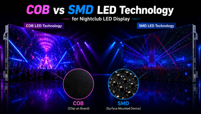
Traditional SMD LEDs use packaged components mounted onto a PCB. Each packaged LED contains multiple structural layers that add height.
COB technology simplifies this structure.
Instead of mounting fully packaged LEDs, COB places LED chips directly onto the circuit board. This eliminates several packaging layers and reduces overall module thickness.
COG takes this concept even further.
Rather than mounting chips onto a PCB, manufacturers place LED chips directly onto glass substrates. This removes one of the thickest structural elements in the display.
Manufacturer Insight
Many marketing materials claim COB automatically produces thinner displays. This is not always true.
We have seen poorly designed COB cabinets exceed the thickness of well-engineered PCB products. Cabinet structure often contributes more thickness than packaging technology alone.
Therefore, buyers should compare complete system dimensions rather than focusing exclusively on packaging terminology.
PCB and Backplane Design
The circuit board itself significantly influences display thickness.
Traditional LED displays typically use rigid FR4 PCBs. These boards provide excellent durability and manufacturing efficiency but add thickness and weight.
Manufacturers can reduce thickness by using:
- Thinner PCB materials
- Flexible circuit structures
- Integrated backplanes
- High-density circuit layouts
However, thinner boards create new engineering challenges.
As thickness decreases, mechanical rigidity decreases as well. This increases the risk of warping during transportation or installation.
Manufacturer Insight
In our production experience, excessive PCB thinning often creates more problems than benefits. Some ultra-thin boards become more vulnerable to thermal deformation after thousands of operating hours.
A slightly thicker board often delivers better long-term reliability.
Power and Signal Integration
Power systems occupy valuable space inside every LED display.
Traditional displays usually contain:
- Power supplies
- Receiving cards
- Hub boards
- Signal distribution systems
Each component adds depth.
Modern manufacturers increasingly integrate these functions into compact modules. This reduces both thickness and installation complexity.
The trend toward integrated electronics plays a major role in ultra-thin display development.
Some fine-pitch indoor displays now use highly integrated architectures that eliminate several traditional internal components.
Cabinet Construction
Cabinet design remains one of the most overlooked thickness factors.
Even if a display uses advanced packaging technology, a poorly designed cabinet can negate those advantages.
A cabinet must provide:
- Structural support
- Precision alignment
- Heat dissipation
- Service access
- Cable management
The challenge lies in balancing these requirements while reducing thickness.
High-end indoor LED displays often use die-cast aluminum cabinets because they provide excellent rigidity with minimal thickness.
Manufacturer Insight
Cabinet design frequently determines whether a display reaches 20 mm or remains above 40 mm.
When our engineers evaluate new ultra-thin concepts, cabinet structure often becomes the limiting factor before LED technology does.
Cooling Requirements
Every LED display generates heat.
As displays become thinner, thermal management becomes more difficult.
A thicker cabinet naturally creates more space for airflow and heat dissipation. Ultra-thin designs reduce this thermal buffer.
This creates a critical engineering challenge.
Manufacturers must balance:
| Design Goal | Engineering Challenge |
| Thinner Structure | Reduced Airflow |
| Lower Weight | Less Thermal Mass |
| Smaller Components | Higher Heat Density |
| Compact Design | More Difficult Maintenance |
Many next-generation COB and COG products rely on improved thermal materials rather than larger cooling systems.
Manufacturer Insight
Heat management becomes significantly more challenging below 20 mm total cabinet depth.
In high-brightness applications, thermal performance often determines long-term reliability more than display thickness itself.
For this reason, experienced buyers should always evaluate thermal design alongside thickness specifications.

Traditional PCB LED Displays Explained
AIO Grab Block
Quick Answer
Traditional LED displays use LEDs mounted on PCB boards, requiring additional structural layers that increase total screen thickness but simplify manufacturing, maintenance, and large-scale production.
| Feature | PCB LED |
| Thickness | 30–80 mm |
| Cost | Low |
| Repairability | High |
| Manufacturing Maturity | High |
| Thinness Potential | Limited |
PCB-based LED displays remain the dominant technology in the global LED industry. Although newer packaging methods attract attention, PCB technology still powers most outdoor billboards, stadium displays, transportation signage, and commercial video walls.
The reason is simple. PCB technology balances performance, cost, scalability, and serviceability better than any other solution currently available.
How PCB-Based LED Displays Are Built
A traditional LED display contains several layers.
The display starts with a PCB substrate. Manufacturers mount SMD LEDs onto the PCB. The PCB then connects to HUB boards, receiving cards, power supplies, and the cabinet structure.
A simplified structure looks like this:
- SMD LED package
- PCB board
- Signal distribution layer
- Power distribution layer
- Cabinet frame
- Mounting structure
Each layer adds thickness.
This layered architecture explains why most traditional LED displays struggle to reach ultra-thin dimensions.
However, those additional layers also provide practical advantages.
For example, technicians can replace individual modules without replacing the entire display surface. This significantly lowers maintenance costs over the display’s lifetime.
Advantages of PCB Technology
Many buyers assume newer technologies automatically replace older technologies.
The LED industry does not work that way.
PCB technology remains relevant because it solves several real-world problems better than emerging alternatives.
Key advantages include:
| Advantage | Benefit |
| Mature Supply Chain | Lower Costs |
| Proven Reliability | Reduced Risk |
| Easy Maintenance | Lower Service Costs |
| High Production Capacity | Faster Delivery |
| Broad Pixel Pitch Range | More Application Options |
From a procurement perspective, PCB displays usually offer the lowest total cost of ownership.
A buyer can often purchase a high-quality PCB display for 20%–40% less than a comparable COB solution, depending on pixel pitch and project scale.
Thickness Limitations of PCB Designs
The biggest drawback of PCB technology is structural thickness.
Even when engineers reduce PCB thickness, the display still requires:
- LED packaging
- Circuit boards
- Connectors
- Internal electronics
- Cabinet reinforcement
As a result, PCB displays typically remain thicker than COB or COG alternatives.
Fine-pitch applications highlight this limitation.
As pixel pitch decreases below P1.5, engineers face increasing difficulty fitting traditional packaged LEDs into compact structures.
This challenge helped drive the development of COB technology.
Manufacturer Insight
Many suppliers advertise ultra-thin PCB displays below 20 mm.
In practice, buyers should carefully review mechanical drawings.
Some manufacturers exclude rear electronics from thickness specifications. Others measure only the display module.
We always recommend requesting:
- Module thickness
- Cabinet thickness
- Installed depth
These three dimensions provide a much more realistic picture.
Common Applications
PCB displays continue to dominate applications where durability, scalability, and serviceability matter more than extreme thinness.
Typical examples include:
- Outdoor advertising billboards
- Stadium LED displays
- Transportation signage
- Rental LED screens
- Command centers
- Shopping mall displays
- Large-format digital signage
For many of these applications, paying a premium for ultra-thin technology provides little practical benefit.
For example, we do not recommend choosing a 10 mm COG display for a 500-square-meter outdoor billboard. The additional cost rarely improves advertising performance.
Instead, budget allocation should focus on brightness, reliability, and maintenance efficiency.
How COB Technology Makes LED Displays Thinner
AIO Grab Block
Quick Answer
COB technology removes traditional LED packaging structures by mounting chips directly onto the PCB, reducing thickness while improving durability, contrast ratio, and fine-pitch performance.
| Feature | COB LED |
| Thickness | 15–35 mm |
| Durability | High |
| Contrast Ratio | High |
| Pixel Pitch | Fine Pitch |
| Repairability | Medium |
COB technology represents one of the most important developments in modern LED display manufacturing.
Instead of packaging LEDs individually before mounting them onto a PCB, COB places bare LED chips directly onto the board surface.
This seemingly simple change removes several structural layers and creates a thinner display architecture.
What Is COB (Chip-on-Board)?
COB stands for Chip-on-Board.
The technology mounts LED chips directly onto a substrate and then protects them using encapsulation materials.
The structure looks like this:
Traditional SMD:
LED Chip → Package → PCB
COB:
LED Chip → PCB
By eliminating the package layer, COB reduces both physical thickness and optical complexity.
The result is a cleaner display surface with improved visual performance.
COB technology has gained significant traction in fine-pitch indoor applications, especially below P1.5.
Structural Differences Between PCB and COB
The key difference lies in the LED packaging process.
| Structure Layer | PCB/SMD | COB |
| LED Package | Required | Eliminated |
| PCB Board | Required | Required |
| Surface Protection | Optional | Integrated |
| Assembly Complexity | Higher | Lower |
| Visual Surface | Discrete LEDs | Continuous Surface |
Removing the package layer reduces the distance between the viewer and the light-emitting chip.
This improves several visual characteristics simultaneously.
Why COB Reduces Display Thickness
The packaging layer contributes significant height in traditional SMD displays.
COB eliminates this layer.
As engineers continue reducing pixel pitch, the benefits become even more apparent.
For example:
| Technology | Typical Fine Pitch Range |
| SMD | P1.2–P2.5 |
| COB | P0.4–P1.5 |
| Micro COB | P0.4–P1.0 |
COB also enables manufacturers to simplify cabinet structures because the display surface becomes more durable.
Less protection means fewer structural components.
Consequently, total cabinet thickness decreases.
Manufacturer Insight
Many buyers focus exclusively on thickness reduction.
However, our engineering team often sees a larger benefit elsewhere.
COB reduces the risk of physical LED damage during transportation and installation.
For large projects, reduced damage rates can save more money than the thickness reduction itself.
Additional Benefits Beyond Thinness
Improved Protection
COB displays create a sealed display surface.
This reduces vulnerability to:
- Dust
- Moisture
- Accidental impact
- Static electricity
Many premium COB products achieve higher protection levels than traditional SMD displays.
Better Black Levels
COB displays typically produce deeper black surfaces.
The continuous surface absorbs ambient light more effectively than individual LED packages.
This improves perceived contrast ratio.
The benefit becomes especially noticeable in:
- Boardrooms
- Broadcast studios
- Luxury retail environments
- Experience centers
Higher Reliability
Reliability remains one of COB’s strongest selling points.
The integrated structure reduces:
- Solder joint exposure
- Mechanical stress
- Physical LED damage
- Maintenance frequency
Manufacturer Insight
One issue rarely discussed online involves repairability.
COB improves durability, but module-level repairs can become more complex than traditional SMD systems.
For buyers managing large display networks, maintenance strategy should be part of the purchasing decision.
Video Placement Recommendation #1
Location: After “Why COB Reduces Display Thickness”
Video Content:
Show a side-by-side comparison of PCB and COB modules. Measure thickness using a digital caliper and demonstrate impact resistance using controlled touch tests.
Purpose:
Help buyers visually understand where thickness reduction actually comes from rather than relying on marketing claims.
Why COG Technology Represents the Next Generation of Ultra-Thin LED Displays
AIO Grab Block
Quick Answer
COG technology replaces conventional PCB substrates with glass, allowing LED chips to be mounted directly onto ultra-thin glass surfaces and achieving the industry’s thinnest commercial LED display structures.
| Feature | COG LED |
| Thickness | 5–10 mm |
| Weight | Very Low |
| Transparency Potential | High |
| Manufacturing Complexity | High |
| Commercial Adoption | Emerging |
If COB removes the LED package, COG removes something even larger.
COG removes the traditional PCB itself.
This structural change creates a fundamentally different display architecture.
As a result, COG currently represents the most promising pathway toward ultra-thin LED displays.
What Is COG (Chip-on-Glass)?
COG stands for Chip-on-Glass.
Instead of mounting LED chips onto FR4 circuit boards, manufacturers place the chips directly onto glass substrates.
The structure becomes:
LED Chip → Glass
This approach dramatically reduces:
- Thickness
- Weight
- Material usage
- Structural complexity
COG technology originally emerged in advanced display applications and now attracts significant interest from Micro LED developers.
How Glass Replaces Traditional PCB Structures
Traditional PCBs perform two jobs:
- Structural support
- Electrical routing
COG replaces both functions using engineered glass substrates with integrated conductive pathways.
Glass provides several advantages:
| Characteristic | Glass Substrate |
| Thickness | Extremely Low |
| Flatness | Excellent |
| Transparency | Available |
| Weight | Low |
| Thermal Expansion Stability | High |
Because glass can be manufactured in extremely thin formats, overall display thickness decreases dramatically.
This explains why many next-generation transparent displays rely on glass-based structures.
Why COG Can Achieve Single-Digit Millimeter Thickness
Several factors contribute.
First, the PCB disappears.
Second, structural layers decrease.
Third, the display surface becomes more integrated.
Combined, these changes allow commercial products to approach thicknesses below 10 mm.
Future Micro LED implementations may eventually approach 5 mm or less.
However, buyers should recognize that achieving laboratory thickness numbers differs from deploying reliable commercial products.
The challenge is not making displays thin.
The challenge is keeping them reliable for years.
Manufacturer Insight
The thinnest display is not always the best display.
In our experience, some ultra-thin prototypes perform well in demonstrations but struggle during transportation, installation, or long-term operation.
Commercial buyers should evaluate lifecycle performance rather than focusing solely on thickness records.
Current Challenges of COG Manufacturing
Despite its advantages, COG faces several barriers.
Yield Rates
Glass-based production requires extremely precise manufacturing.
Small defects can significantly impact yield.
Production Costs
COG production remains more expensive than PCB and COB manufacturing.
The technology still lacks the scale advantages of mature PCB supply chains.
Repair Complexity
Field repairs become more difficult.
Replacing damaged glass-based structures often requires specialized procedures.
Supply Chain Maturity
The ecosystem remains smaller than traditional LED manufacturing.
Many suppliers continue investing heavily in process optimization before large-scale adoption.
Manufacturer Insight
Today, we view COG as a premium technology rather than a mainstream replacement.
For luxury retail, fine-pitch visualization, transparent displays, and future Micro LED applications, COG offers compelling advantages.
For many standard commercial projects, PCB and COB still provide stronger value per dollar invested.

PCB vs COB vs COG: Thickness Comparison From a Manufacturing Perspective
AIO Grab Block
Quick Answer
The largest reduction in LED display thickness comes from eliminating structural layers. PCB uses multiple layers, COB removes LED packaging layers, and COG removes the PCB itself.
| Factor | PCB | COB | COG |
| Thickness | Thickest | Medium | Thinnest |
| Weight | High | Medium | Low |
| Cost | Lowest | Medium | |
| Highest | |||
| Repairability | Best | Good | Limited |
| Production Complexity | Low | Medium | High |
Many online comparisons stop at technical definitions. However, procurement teams need a manufacturing perspective because production decisions directly affect project cost, lead time, maintenance, and long-term reliability.
From our experience as an LED display manufacturer, thickness is not determined by one component. It is the result of hundreds of engineering trade-offs made during product development.
Layer-by-Layer Structure Comparison
The easiest way to understand thickness differences is to compare structural layers.
| Structure Layer | PCB | COB | COG |
| LED Package | Yes | No | No |
| PCB Substrate | Yes | Yes | No |
| Glass Substrate | No | No | Yes |
| Protective Coating | Optional | Yes | Yes |
| Cabinet Structure | Yes | Yes | Minimal |
| Power System | Yes | Yes | Integrated |
Each eliminated layer contributes to a thinner display.
However, eliminating layers also removes safety margins.
Traditional PCB designs tolerate mechanical stress well because the structure contains multiple protective layers. COG designs reduce those layers to achieve thinner profiles.
This explains why engineering complexity increases as thickness decreases.
Weight Comparison
Weight reduction often matters more than thickness.
Architects frequently focus on depth because it is visible. Structural engineers usually focus on weight because it affects building loads.
The relationship is straightforward.
Less material equals less weight.
| Technology | Typical Weight Reduction vs PCB |
| COB | 10–25% |
| COG | 30–50% |
| Future Glass-Based Micro LED | 40–60% |
For large projects, these differences become significant.
A 200-square-meter display weighing 30% less can reduce transportation costs, simplify installation, and lower structural reinforcement requirements.
Manufacturer Insight
Many clients initially ask about thickness.
After engineering evaluation, weight often becomes the more important parameter.
For suspended installations such as airports, exhibition halls, and transportation hubs, reducing weight frequently delivers more value than reducing thickness.
Installation Impact
Thin displays create installation advantages.
Benefits include:
- Reduced wall projection
- Improved architectural integration
- Easier concealment
- Cleaner aesthetics
- Greater design flexibility
However, installation complexity does not always decrease.
Ultra-thin systems often require tighter installation tolerances because structural rigidity decreases as thickness decreases.
This means installers must work with greater precision.
A Practical Example
Consider a luxury retail project.
A traditional 60 mm display may visibly protrude from a wall.
A 10 mm COG display can create a nearly flush appearance.
In this scenario, paying more for reduced thickness may justify the investment because aesthetics directly influence customer perception.
Transportation Impact
Transportation damage remains one of the most overlooked cost drivers in LED projects.
Thinner displays reduce shipping volume.
However, thinner structures can also become more vulnerable during handling.
| Transportation Factor | PCB | COB | COG |
| Shipping Volume | High | Medium | Low |
| Impact Resistance | Good | Excellent | Moderate |
| Packaging Requirement | Standard | Standard | Enhanced |
| Damage Risk | Medium | Low | Higher |
Manufacturer Insight
COB often achieves the best balance between thinness and transportation durability.
Its encapsulated surface protects LED chips from accidental contact during shipping and installation.
This is one reason why many fine-pitch commercial projects currently favor COB rather than COG.
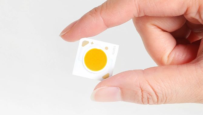
Does a Thinner LED Display Always Mean a Better Display?
AIO Grab Block
Quick Answer
No. The best LED display depends on application requirements. Ultra-thin designs improve aesthetics and installation flexibility but often increase cost, complexity, and maintenance requirements.
| Consideration | Thin Display | Standard Display |
| Appearance | Better | Good |
| Installation Space | Better | Good |
| Cost | Higher | Lower |
| Repairability | Lower | Higher |
| Structural Strength | Design Dependent | Usually Higher |
One of the biggest mistakes we see in procurement discussions is assuming thinner automatically means better.
This assumption often leads to unnecessary spending.
Buyers should evaluate whether reduced thickness creates measurable business value.
If it does not, that budget may produce greater returns elsewhere.
Trade-Off Between Thinness and Cost
Ultra-thin technology requires more advanced manufacturing.
The process often involves:
- Tighter tolerances
- Specialized materials
- Higher yield requirements
- More complex quality control
Consequently, costs increase.
| Technology | Relative Cost |
| PCB | 1.0x |
| COB | 1.2–1.8x |
| COG | 2–4x |
These figures vary by pixel pitch and project size, but the trend remains consistent.
Reverse Recommendation
We do not recommend choosing a COG display solely because it is thinner.
If the installation environment provides sufficient depth, the additional investment may not improve user experience.
For many conference rooms, control rooms, and retail displays, a COB solution delivers a better cost-performance ratio.
Trade-Off Between Thinness and Serviceability
Maintenance often receives less attention during procurement.
However, maintenance costs continue for years after installation.
Traditional PCB displays offer excellent serviceability because technicians can replace modules quickly.
COB introduces additional repair complexity.
COG may require specialized repair procedures depending on product architecture.
| Technology | Maintenance Convenience |
| PCB | Excellent |
| COB | Good |
| COG | Moderate to Limited |
Manufacturer Insight
Many buyers underestimate maintenance costs.
Over a seven- to ten-year lifecycle, maintenance expenses can exceed the initial thickness premium of advanced display technologies.
This is especially true for large display networks.
When Ultra-Thin Displays Make Sense
Ultra-thin displays create genuine value in specific applications.
Examples include:
- Luxury retail storefronts
- Corporate experience centers
- Museums
- High-end showrooms
- Glass-integrated displays
- Architectural media installations
These projects often prioritize aesthetics and space efficiency.
In such cases, thickness becomes part of the customer experience.
When Traditional Structures Remain Better
Traditional PCB and COB solutions often remain the smarter choice.
Applications include:
- Outdoor billboards
- Stadium displays
- Transportation signage
- Rental displays
- Large public information systems
For these projects, brightness, durability, and maintenance efficiency usually matter more than thickness.
Reverse Recommendation
We do not recommend pursuing a 10 mm display for a stadium scoreboard viewed from 100 meters away.
The audience will never notice the thickness difference.
The budget would generate a better return if invested in:
- Higher brightness
- Better calibration
- Redundant power systems
- Higher refresh rates
Video Placement Recommendation #2
Location: After “When Ultra-Thin Displays Make Sense”
Video Content:
Show two real-world installations:
- Ultra-thin retail display integrated into a luxury storefront.
- Traditional LED display installed in a stadium environment.
Highlight why thickness matters in one scenario and becomes irrelevant in the other.
Purpose:
Help buyers understand that application requirements should drive technology selection.
How to Choose the Right LED Technology for Your Project
Technology selection should begin with application requirements rather than marketing claims.
The best display is not necessarily the thinnest display.
The best display is the one that delivers the required performance at the lowest lifecycle cost.
Choose PCB If
PCB technology remains the best option when you need:
- Large display areas
- Outdoor installations
- Stadium applications
- Rental LED screens
- Easy maintenance
- Maximum budget efficiency
Typical projects include billboards, transportation displays, and sports venues.
Choose COB If
COB technology works best when you need:
- Fine-pitch LED video walls
- Better contrast ratios
- Enhanced durability
- Reduced thickness
- Premium indoor environments
Typical projects include:
- Corporate lobbies
- Command centers
- Boardrooms
- Broadcast studios
- Experience centers
For many indoor projects, COB currently offers the best balance between performance and cost.
Choose COG If
COG becomes attractive when your project prioritizes:
- Ultra-thin architecture
- Glass integration
- Premium design aesthetics
- Transparent displays
- Future Micro LED deployment
Typical projects include:
- Luxury retail environments
- High-end showrooms
- Smart buildings
- Museum installations
- Advanced visualization systems
Reverse Recommendation
We do not recommend selecting COG solely because it represents the newest technology.
If thickness does not create measurable value for your project, a COB solution often delivers stronger ROI.
Decision Matrix for Buyers
| Project Requirement | Recommended Technology |
| Lowest Cost | PCB |
| Outdoor Durability | PCB |
| Best Maintenance Access | PCB |
| Fine Pitch Video Wall | COB |
| Better Contrast Ratio | COB |
| High-Traffic Indoor Space | COB |
| Ultra-Thin Design | COG |
| Transparent Display | COG |
| Architectural Integration | COG |
Conclusion
PCB, COB, and COG technologies each serve different purposes. PCB remains the most practical choice for large-scale and cost-sensitive projects, COB offers an excellent balance of thinness and performance, while COG represents the future of ultra-thin and glass-based display solutions.
The best LED display is not necessarily the thinnest one. Buyers should evaluate thickness alongside installation requirements, maintenance strategy, and total project cost to achieve the best long-term value.
Need help choosing the right LED display technology? Contact NSELED for expert project consultation and customized LED display solutions tailored to your application.